-
Corporate
 Thai Parkerizing is a leader in Heat & Surface treatment business.
 -
Chemical Products
 Surface treatment chemicals for a diverse range of purposes with our extensive technical supports.
 -
Processing Services
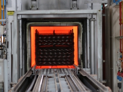 Various kind of heat and surface treatment services to fulfill customer requirements with high quality systems.
 -
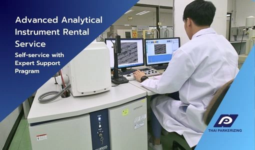
Laboratory Services
 Thai Parkerizing Analysis Center is an analysis and testing laboratory in chemical, metallurgical and environmental fields.
 - Articles
- Contact us
What is EDS? EDX Analysis with a Scanning Electron Microscope
Not only the EU countries have strict production control standards in terms of safety, health and the environment. Manufacturing industry in Thailand also has raised the production process standards with stricter health and hygiene measures. Therefore, in manufacturing industries and factories, a procedure for testing and analyzing product material compositions and chemical contaminants in a detailed manner is required, which is the area where chemical composition analysis services come into play.
Chemical Composition and Microstructure Analysis: A Comprehensive Guide
A material's microstructure comprises a variety of distinct phases. Each has a different shape, size, and distribution (grains, precipitates, dendrites, spherulites, lamellae, pores, etc.). With an optical or electron microscope, the different crystalline, semi-crystalline, or amorphous structures of the phases may be seen. Controlled microstructural alterations made during processing allow the engineer to achieve various attributes.
Chemical Composition and Microstructure Analysis: A Comprehensive Guide

A material's microstructure comprises a variety of distinct phases. Each has a different shape, size, and distribution (grains, precipitates, dendrites, spherulites, lamellae, pores, etc.). With an optical or electron microscope, the different crystalline, semi-crystalline, or amorphous structures of the phases may be seen. Controlled microstructural alterations made during processing allow the engineer to achieve various attributes.
Spectroscopy Instrumentation
Chemical Composition Analysis can be performed using advanced elemental and compound analysis tools. Which is the most suitable method? It depends on the type of sample material to be analyzed. One of the most popular methods in industrial labs is the use of various spectrometer instruments and different techniques.
- FT-IR Spectroscopy (Fourier Transform Infrared Spectroscopy)
Mathematical processes are used to convert the raw data (interferogram) into the entire spectrum of the infrared rays. The FTIR technique may obtain a fuel sample's infrared transmission or absorption spectra. Organic and inorganic substances may be identified using FTIR.
In nanoparticle surface analysis, FTIR is an excellent choice of instrument. The surface chemical composition of NPs may be assessed under particular circumstances, and the reactive surface sites responsible for the surface reactivity are discovered. - Emission Spectrum
In chemistry, the emission spectrum refers to the range of electromagnetic radiation frequencies released when an electron transitions from high-energy to low-energy. The emitted photon's photon energy is equal to the difference in energy between the two states. Each atom has several possible electron transitions, and each change has a distinct variation in power.
What Are The Many Types Of Microscopes?
Aside from the use of spectrometer instruments, various types of microscopes are also used to analyze microscopical structures.
- Optical Microscope; OM
This microscope, also known as a light microscope, employs visible light and a series of lenses to produce magnified pictures of tiny objects. Optical microscopes may have been created in the 17th century in their current complex form. - Confocal Laser Scanning microscope; CLSM
One of the most significant advancements in fluorescence imaging in recent decades has been the development of CLSM, which is now widely regarded as a necessary tool in biological research. Because of the reduced specimen preparation required and compatibility with three-dimensional (3D) live imaging, CLSM provides better access to dynamic cellular and molecular processes than electron microscopy. - Transmission Electron Microscopy; TEM
When it comes to analyzing a wide variety of materials, electron microscopes have proven to be an invaluable resource. Because of their excellent spatial resolution and adaptability are a handy tool for a wide range of applications. Transmission electron microscope (TEM) and scanning electron microscope (SEM) are the two most common kinds of electron microscopes (SEM). - Scanning Electron Microscope; SEM
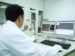
The Thermo Scientific Prisma E Scanning Electron Microscope (SEM) combines various imaging and analytical modalities with sophisticated automation to provide the most comprehensive solution in its class. Applications in industrial research and development, quality control, and failure analysis that demand high-resolution imaging with sample flexibility and an intuitive user interface are suited for this instrument.
What is Scanning Electron Microscope; SEM
Electron microscopes that employ a focused stream of electrons to create pictures are known as scanning electron microscopes (SEM). The sample's surface topography and composition are revealed via the signals generated by the electrons' interactions with the sample's atoms.
How Does SEM-EDX Analysis Work?

When an electron beam strikes an atom's inner shell, it knocks one electron out and leaves a positively charged electron-hole. This is how EDX analysis works. Displacement of an electron causes an outer shell electron to be drawn into the void and fill it. An X-ray can be produced when an electron moves from the outer higher-energy shell to the inner lower-energy surface of an atom.
When the process generates X-rays, a silicon drift detector collects them and uses software to analyze the signal. Elemental mapping and line scanning are two standard methods for depicting chemical data. Using X-rays, each element in a sample may be identified in this manner.
When the process generates X-rays, a silicon drift detector collects them and uses software to analyze the signal. Elemental mapping and line scanning are two standard methods for depicting chemical data. Using X-rays, each element in a sample may be identified in this manner.
Utilizing the SEM/ EDS Microscope System Energy Dispersive Spectronomy)
A core-shell electron is ejected from a material that has been energized by an energy source (such as the electron beam of an electron microscope). A higher-energy outer-shell electron then takes its place, releasing the difference in energy as an X-ray with a distinct spectrum dependent on the atom from which it originated.
Conclusion
When an electron beam strikes an atom's inner shell, it knocks one electron out and leaves a positively charged electron-hole. This is how EDX analysis works. Using X-rays, each element in a sample may be identified in this manner. The two most common kinds of electron microscopes (SEM) are TEM and SEM. SEM's high-resolution imaging and intuitive user interface are suited for a wide variety of scientific and industrial applications.
Finally, if you are looking for a chemical analysis to do material or product tests for your projects, Thai Parkerizing’s expertises carry out advanced chemical analysis in our laboratories to create effective solutions for customer needs. Our wide range of testing services include chemical analysis, surface and metallurgical analysis and various testings.
Related products