- Corporate
- Chemical Products
- Chemical Controller
- Chemical for Paint Booth
- Coil Coating
- Degreasing and Cleaning chemical
- Heat&Cool exchanger (PLATECOIL)
- Hydrophilic
- Manganese Phosphate
- Nano-coating (Pallucid)
- Rolling Oil
- Rust Preventive Product
- Stearate Soap Lubricant/Dry-in-Place Lubricant (PULS)
- Trivalent Chromium/Non-Chromium
- Zinc Phosphate/Iron Phosphate
- Processing Services
- Laboratory Services
- Articles
- What's New
- Contact Us
- Privacy Policy
- E-Service
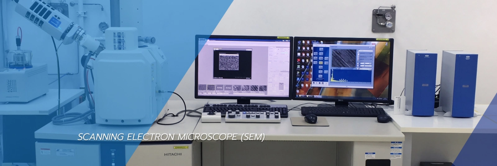
Scanning Electron Microscope (SEM)
Details
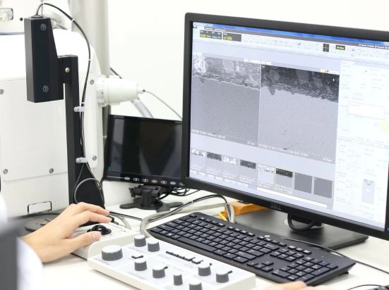
Scanning Electron Microscope (SEM) is an advanced tool for inspecting and analyzing the surface of materials at the micrometer level. It uses a focused electron beam to scan the sample surface and generate high-resolution images, displaying both Secondary Electron (SE) images and Backscattered Electron (BSE) images.
Additionally, the SEM can be equipped with Energy Dispersive Spectroscopy (EDS) or EDX for chemical composition analysis, enabling:
- Point Analysis
- Line scan Analysis
- Mapping Analysis
Sample Analysis Services
- SEM Imaging Service: Magnification range from 40x to 100,000x.
- Sample Types: Solid, powder, and non-conductive materials.
- Material Analysis: Metals, alloys, plastics, polymers, and natural fibers.
- Chemical Composition Analysis: Point Analysis, Line scan analysis and mapping analysis
Usage Limitations
- The sample must be oil-free.
- The sample must be moisture-free.
- The sample weight must not exceed 500 g.
- The sample dimensions must not exceed 120 mm x 50 mm (width x height).


